1. Pulse Operation Schemes for Humidity Sensing
The humidity-sensing properties of the sensor are
demonstrated using pulse operation schemes. Figs. 3(a)
and 3(b) show the pulse signal waveforms for operating
the sensor to obtain the pulsed $I_D-V_{CG}$ (PIV) characteristics
and the transient $I_D$ behaviors, respectively. The CG
bias ($V_{CG}$) is swept ranging from 2 to -2 V for PIV measurement,
while a fixed value of -0.2 V is applied to the
CG read bias ($V_{rCG}$) for transient ID measurement. For
both PIV and transient $I_D$ measurements, the base voltages
($V_{bases}$) of the CG and drain pulses are fixed at 0 V, and the drain read bias is -0.1 V. A single pulse signal
is applied to the CG terminal with the high and low levels
corresponding to $V_{CG} (or V_{rCG})$ and $V_{base}$, respectively. The
durations of the high and low levels are defined as ton and
toff, respectively, which are set to 30 μs and 100 ms in this
study. The drain pulse signal is synchronized with the CG
pulse signal, following the same timing scheme.
The pulse operation scheme in Fig. 3(b) has been previously
proposed and its effect has been verified [
27]. According
to [
27], through the application of a pulse operation
scheme, the ID drift of a Si FET-type sensor caused
by the DC bias is significantly reduced, which facilitates
the obtaining of stable sensing characteristics.
Fig. 4 displays the transfer ($I_D-V_{CG}$) characteristics of
the fabricated FET-type humidity sensor. The channel
width and length of the FET are both 2 mm. The $I_D-V_{CG}$
curves are measured at an RH of 3.4% and room temperature
using the DC and PIV methods. The two logarithmic
$I_D-V_{CG}$ curves obtained by the DC and PIV methods coincide
well with each other at |$I_D$| > 1 nA. This implies that
the $t_{on}$ of 30 ms is appropriate to operate normally the FET
of the humidity sensor.
Pulse signal waveforms for operating the humidity sensor to measure (a) PIV and (b) transient $I_D$ behavior.
DC and PIV characteristics of the humidity sensor.
2. Chemical Reaction and Chemical-to-electrical Transduction Mechanisms
Fig. 5(a) shows the shift in the $I_D-V_{CG}$ curves of the sensor
obtained using the PIV method with varying RH inside
the test chamber. Each $I_D-V_{CG}$ curve is measured 300 s after
injecting $N_2$ gas with a certain RH into the test chamber
to saturate the ambient RH inside the test chamber.
Fig. 5(b) illustrates the variation of threshold voltage ($V_{th}$)
with respect to RH.$V_{th}$ is extracted from each $I_D-V_{CG}$ curve
in Fig. 5(a) using the linear extrapolation method. The increase in RH from 3.4% to 80.3% leads to the change in
$V_{th}$ (△$V_{th}$) by -134 mV.
Here, we explain the reason for the △$V_{th}$ being negative
with the increase of RH. As shown in Fig. 6, adsorption
of water molecules onto the surface of the $WO_3$ humiditysensing
layer is divided into two steps. At a lower RH,
water molecules dissociate into hydroxide (OH-) and hydrogen
(H+) ions when exposed to the WO3 layer [
28].
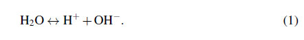
The OH- ions interact with the tungsten cations on
the $WO_3$ surface. Whereas, the H+ ions interact with the
lattice oxygens or the oxygen ions existing on the surface
of the WO3 layer, forming the hydroxyl groups that
are chemically bonded to the tungsten cations [28]. Finally,
both OH- and H+ ions are chemically adsorbed
(chemisorbed) onto the surface of the WO3 layer in the
form of a hydroxyl group (-OH). Note that the O-H
chemical bond in this hydroxyl group is a polar covalent bond with the negatively polarized oxygen atom and the
positively polarized hydrogen atom.
Meanwhile, we must recall a fact that has already been
demonstrated experimentally in our previous study [18].
In [18], it was revealed that the sensor response changes
depending on the pre-bias ($V_{pre}$) applied to the CG. When
$V_{pre}$ is negative, the electrons of the ZnO sensing layer
are accumulated near the interface between the ZnO layer
and the O/N/O layer, and the chemical reaction between
NO2 (target gas) and ZnO mainly occurs near the interface,
which is relatively close to the FET channel. Therefore,
the sensor response increases compared to that in the
case of $V_{pre}$ = 0 V. However, when $V_{pre}$ is positive, the
ZnO layer near the interface is depleted. Consequently, the
chemical reaction mostly happens in the bulk region of the
ZnO layer. In this case, the sensor response eventually decreases
compared to that in the case of $V_{pre}$ = 0 V because
the amount of chemical reaction at the interface between
the ZnO layer and the O/N/O layer is reduced due to the
depletion of the ZnO layer. In summary, the chemical reaction
occurring in the sensing layer near the interface between
the sensing layer and the O/N/O layer dominantly
affects the FET of the sensor. Therefore, in this study, it
is assumed that the chemical reaction between $H_2O$ and
$WO_3$ occurs predominantly near the interface between the
$WO_3$ layer and the O/N/O layer.
At the interface between the $WO_3$ layer and the O/N/O
layer near the FG, the positively polarized hydrogen atoms
of the hydroxyl groups generated by $H_2O$ chemisorption
on the$WO_3$ layer induce a negative sheet charge at the
interface of the FG in contact with the O/N/O layer. This
negative sheet charge consists of the electrons, which are
the majority carriers of the n-type poly-Si FG. Simultaneously,
a positive sheet charge, which consists of the depletion
charge of the n-type poly-Si FG, is induced at the interface of the FG in contact with the gate oxide. This positive
sheet charge reduces the hole concentration of the ptype
FET channel of the sensor. In summary, chemisorption
of water molecules onto the surface of the $WO_3$ layer
shifts Vth of the p-type FET sensor in the negative direction,
causing |$I_D$| to decrease. At a higher RH, additional
water molecules are physically adsorbed (physisorbed)
onto the hydroxyl groups formed by chemisorption of water
molecules [28]. The first physisorbed layer of water
molecules are formed by the hydrogen bond between the
hydrogen atoms of the hydroxyl groups already bonded
to the $WO_3$ layer via chemisorption of water molecules
at a lower RH, and the oxygen atoms of the additional
water molecules [28]. From the second physisorbed layer,
hydrogen bonds occur between the hydrogen atoms of
the previously physisorbed water molecules and the oxygen
atoms of added water molecules [28]. Similar to the
chemisorbed layer, the molecular arrangement of these
multiple physisorbed layers can be regarded as a dipole
with the direction of the dipole moment being toward the
FET channel of the sensor, thereby reducing the hole concentration
of the channel. Therefore, $V_{th}$ and |$I_D$| of the
sensor decrease as RH increases, regardless of whether
water molecules are chemisorbed or physisorbed onto the
surface of the $WO_3$ layer.
(a) $I_D-V_{CG}$ characteristics of the humidity sensor as a function of relative humidity ranging from 3.4% to 80.3% measured by using the PIV method. (b) Variation of $V_{th}$ with RH.
Schematic diagram of adsorption of water molecules on the $WO_3$ sensing layer.
3. Change of Energy Band Structure during Humidity Sensing
Next, we examine the change in energy band structure
of the sensor when water molecules are adsorbed onto
the WO3 sensing layer. Fig. 7(a) shows the schematic energy
band diagram of the sensor under flat-band condition.
Here, $Φ_{CG}, Φ_{WO3}, Φ_{FG}$, and $Φ_{sub}$ represent the work
functions of CG,$WO_3$ sensing layer, FG, and Si substrate,
respectively. $χ_{WO3}$, $χ_{FG}$, and $χ_{sub}$ stand for the electron affinities of $WO_3$ sensing layer, FG, and Si substrate, respectively.
Because the Au of the CG occupies most of
the direct contact area with the $WO_3$ layer, the $Φ_{CG}$ is regarded
as the work function of Au (5.1 eV). The electron
concentrations of the FG and the substrate are ~1x10$^21$
and ~1x10$^16$ cm$^{-3}$, respectively, thus the FFG and the
Fsub are ~4.05 and ~4.26 eV, respectively. $WO_3$ is a wellknown
n-type semiconductor [
29] with an $χ_{WO3}$ value of
~3.3 eV [
30]. The $χ_{FG}$ and the $χ_{sub}$ are both 4.05 eV. Note
that the FG is in a fresh state, as shown in Fig. 7(a). This
implies that electrons or holes are not stored in the FG.
Fig. 7(b) shows the schematic energy band diagram under
equilibrium condition where all the electrodes in the sensor
are grounded (0 V). As the |$I_D$| at $V_{CG}$ = 0 V is ~0.2
μA in the $I_D-V_{CG}$ curve in Fig. 4, it can be inferred that the
FET of the sensor is in weak inversion. In addition, considering
the band structure shown in Fig. 7(a), it is evident
that electrons are initially stored in the FG, as shown in
Fig. 7(b). This phenomenon is similar to the programmed
state of a flash memory device with a poly-Si floatinggate;
we have confirmed the program and erase characteristics
of the sensor in the previous study [
18]. Fig. 7(c)
illustrates the change of the energy band diagram before
and after humidity sensing at $V_{CG} = V_{rCG}$ = -0.2 V. As
described in Fig. 6, the chemical reaction between water
molecules and the $WO_3$ sensing layer results in the formation
of hydroxyl groups by chemisorption or dipoles by
physisorption at the interface between the WO3 layer and
the O/N/O layer. These hydroxyl groups and dipoles both
exhibit the dipole moments in the same direction from
the interface to the FET channel. This induces a negative
sheet charge at one interface of the FG in contact with the
O/N/O layer and a positive sheet charge at the opposite interface
of the FG in contact with the gate oxide. The localization
of these charges results in a change in the electric
field, which consequently decreases |$I_D$| of the FET.
4. Sensor Response as a Function of Relative Humidity
Fig. 8(a) shows the transient $I_D$ behaviors as a parameter
of RH using the pulse measurement method presented in
Fig. 3(b). Similar to the experimental method used when
obtaining the results shown in Fig. 5, $N_2$ gas with a certain
RH is injected into the test chamber for 300 s to saturate
the humidity sensing before the pulse biases are applied
to the sensor for 10 s to measure every transient $I_D$ curve.
At this time, the $V_{rCG}$ and the $V_{rDS}$ are -0.2 V and -0.1
V, respectively. $I_D$ decreases with the increase in RH and there is no drift in any of the transient $I_D$ curves owing
to the pulse measurement method. In the previous studies
[31,32], drifts in output signals have been observed due
to the application of DC bias to the sensors, which are
undesirable because they degrade the accuracy of sensing
and therefore induce errors in sensor operations. However,
this study confirms that the pulse bias to the sensor
can suppress $I_D$ drift. This method also offers the advantage of reduced power consumption during operation. Fig.
8(b) shows the sensor response (R) versus RH calculated
from the $I_Ds$ in Fig. 8(a), where R is defined as the rate
of change in $I_D$ divided by $I_D$ at an RH of 3.4%. The Rs
are 22.3% and 45.5% at RHs of 54.9% and 80.3%, respectively.
As RH increases from 3.4% to 54.9%, R increases
and then appears to saturate. However, it linearly
increases above an RH of 54.9%. It is speculated that a
change in the adsorption process of water molecules on
the WO3 layer from chemisorption to physisorption occurs
at this inflection point (RH = ~54.9%), which needs
to be proven through further research.
The dynamic response of the sensor is also demonstrated
in Fig. 9 via the injection of $N_2$ gas with a certain RH and the reference $N_2$ gas with an RH of 3.4% alternately
into the test chamber for 180 and 300 s, respectively.
To measure the transient $I_D$ curve for the dynamic
response, $N_2$ gases with RHs of 11.5%, 28.2%, 54.9%,
and 68.5% are sequentially injected, and the reference $N_2$
gas is injected for sensor recovery. The $V_{rCG}$ and the $V_{rDS}$
are -0.2 V and -0.1 V, respectively. Similar to the results
shown in Fig. 8(a), |$I_D$| decreases with the increase in RH
of the injected $N_2$ gas. The response and recovery speeds
of the sensor are also obtained by defining response time
as a time duration for which |$I_D$| decreases by 90% of the
change in $I_D$ during response, and recovery time as a time
duration for which |$I_D$| increases by 90% of the change in
$I_D$ during recovery. The response and recovery times of the
sensor are 97 and 190 s, respectively, at an RH of 68.5%.
Schematic band diagrams at (a) flat-band condition, (b)
equilibrium condition ($V_{CG}$ = 0 V) and (c) the read bias
($V_{CG} = V_{rCG}$ = -0.2 V). In (c), the gray and the black
lines stand for the states before and after humidity sensing,
respectively.
(a) Transient ID behaviors of the humidity sensor as a parameter of relative humidity ranging from 3.4% to 80.3%. Each curve is obtained by adopting the pulse scheme explained in Fig. 3(b) for 10 s. (b) R versus relative humidity.
Dynamic response of the humidity sensor monitored by
changing relative humidity of the injected $N_2$ carrier gas.
The relative humidity of the dry $N_2$ gas for recovery is
3.4%.