Metal Oxide Resistive Memory Modeling with Physical Current Equation
I. INTRODUCTION▼
Resistive-Switching Random-Access Memory (ReRAM)
is a next-generation non-volatile memory device with
compatible with CMOS process, fast switching time and
low program voltage with a Metal-Insulator-Metal (MIM)
structure [1]. Bipolar ReRAM consists of two terminals
and stores data by controlling between a low resistance
state (LRS) and a high resistance state (HRS). These states
are achieved by controlling the formation and recombination
of conductive filaments (CF) through the continuous
arrangement of oxygen ion vacancy by voltage applica-tion. Due to these advantages and the characteristic of
outputting current by controlling resistance through CF
formation, ReRAM is employed in arrays to represent
weights in neuromorphic and AI computing fields.
In this paper, we developed a Verilog-A model that
can be directly applied to array simulations. The model
selected and employed a formula primarily focused on
current conduction from the available current formulas
for quick simulation [2-4]. To validate the model, we calibrated
it using experimental data reported for two types
of ReRAM devices. The first device utilized $SiN_x$ as the
switching layer [5]. The $SiN_x$ layer exhibited pores with
an average size of 30 nm, distributed within a range of 20
to 50 nm. These structural characteristics were reported to
minimize randomness in CF formation, resulting in more
consistent device operation. The second device utilized
$HfO_x$ as the switching layer, along with an additional Ge-
Sb-Te (GST) layer to enhance CF stability [6]. While the
thin $HfO_x$ layer could potentially increase randomness
during operation, the GST layer was shown to mitigate
this by localizing CF formation.
II. VERILOG – A COMPACT MODEL FOR
RERAM▼
The flow of current during the operation of ReRAM
is ultimately determined by the formation of CF and the
electron tunneling distance gap determined accordingly.
In this model, the calculation of the gap used an existing
formula that simplifies the formation of CF (1). Additionally,
the conduction of current is expressed using
the following four Eqs. (2)-(5): Schottky emission, Poole-
Frenkel (P-F) emission, space-charge-limited conduction
(SCLC), and trap-assisted tunneling (TAT), in that order.
Furthermore, since the thickness of the device with the
thinnest switching layer among the two modeled devices
is 10 nm (with both the Ge-Te-Se layer and the $HfO_x$ layer
measuring 10 nm), formulas related to direct tunneling
and Fowler-Nordheim (FN) tunneling were not employed.
In ReRAM, the dominant formula for current in the HRS
and LRS varies depending on the type of switching layer.
Each equation shows a current output value with a unique
slope according to the input voltage according to the physical
properties. Accordingly, when determining the output
current value in the model, the measured value was divided
into HRS and LRS parts, and the current formula
with a similar slope to the measured current value was
designated as the dominant equation.
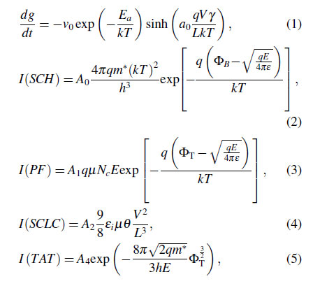
where, $E_a$ is the activation energy for oxygen ions to generate
or recombine the vacancy, L is switching layer thickness
, a0 is atomic hopping site distance, E is electric field
applied to the device, μ is electron mobility in the switching
layer, $N_c$ is the density of states in the conduction band,
$m^∗$ is electron effective mass in the switching layer, $Φ_B$ is
junction barrier height, $Φ_T$ is electron trap energy at the edge of the conduction band, θ is the ratio of free and
shallow trapped charge, and γ, v0, A1, A2, A3, A4 are fitting
parameters [2,3,7].
Ⅲ. SELECTION OF MAJOR CURRENT EQUATION▼
As mentioned in the previous paragraph, when the
physical properties of the current equation are input, all
equations have a constant slope regardless of the fitting
parameters.
Fig. 1 compares the measured output of 10 DC cycles
for a $SiN_x$ based ReRAM device with calculated values
derived from various current equations. Consistent with
prior studies [8], the output current in ReRAM devices follows
a dominant current equation. To identify the most appropriate
equation, the SET/RESET process was divided
into HRS and LRS regions, and the equation with the closest
slope to the measured data was selected. This approach
reduced computational complexity, making it efficient for
large scale array simulations while maintaining accuracy.
For HRS modeling, the P-F Emission equation provided
the best fit, with TAT added to enhance accuracy in the
SET-HRS region. The SET-LRS region was modeled using
the P-F Emission equation, ensuring alignment with
experimental results.
The model parameters were assigned on the basis of the
fabrication characteristics, which are outlined in the following
list: $Φ_B$ = 0.7 eV, $Φ_T$ = 0.3 eV, θ = 0.1, insulator
carrier mobility = 0.1 $cm^2$/Vs, $SiN_x$ relative permittivity
= 7, and effective carrier mass ($m_e$) = 0.5$m_o$ [9-13].
Modeling of SET operation according to the current
equation of a ReRAM device with SiNx as a switching
layer.
Modeling of SET operation according to the current
equation of a ReRAM device with $HfO_x$ and Ge-Se-Te as a switching layer [6].
Fig. 2 illustrates the modeling of a ReRAM device that
incorporates $HfO_x$ and Ge-Se-Te layers as the switching
layer to ensure stable state conversion. Unlike the $SiN_x$
based device, which is modeled with a single current equation,
the thin switching layer and the GST layer in this
device necessitate the use of combined current equations
for accurate modeling. In the HRS region, the Schottky
Emission formula was applied for low-voltage conditions,
while the P-F Emission formula was utilized for highvoltage
conditions. In the LRS region, the current output
was modeled by integrating the Schottky Emission and
SCLC formulas, represented as the cyan curve in the figure.
This approach demonstrates that devices with complex
switching layers can be effectively modeled using a
combination of multiple current equations.
The parameters used in the model include a $HfO_x$ insulator
permittivity of 22, an insulator carrier mobility of
$4×10^{−12} cm^2/Vs$, $m_e = 0.5m_o$, and $Φ_B$ = 0.7 eV [14-16].
In the case of Fig. 3(a), the device utilizes $SiN_x$ as a
switching layer, and the measured and modeled values can
be calibrated using only a single current equation. Therefore,
both HRS and LRS in SET can be modeled using
the P-F Emission equation, and in RESET, HRS is modeled
using the P-F Emission equation, and LRS is modeled
using the equations of SCLC. Also, in the case of
Fig. 3(b), $HfO_x$ and Ge-Se-Te layers were used as switching
layers, so modeling could not be performed using only
one current equation. Accordingly, modeling was carried
out by outputting the sum of the two current equations.
For the SET process, HRS was modeled using Schottky Emission and P-F Emission equations, and LRS was modeled
using Schottky Emission and SCLC equations. During
the RESET process, P-F Emission equation was used
for HRS, Schottky emission and SCLC equations were
used for LRS below −1 V, and only Schottky Emission
equation was used for −1 V and above.
(a) ReRAM device modeling using $SiN_x$ layer as switching
layer. (b) ReRAM device modeling using $HfO_x$ and Ge-Se-Te as switching layers [7].
IV. CONCLUSION
▼
In this study, we developed a voltage-current density
equation for ReRAM modeling, which can be automatically
selected based on the gap width and implemented using
Verilog-A for efficient large-scale SPICE simulations.
It was found that once the material properties are determined,
adjusting the fitting parameters does not change
the slope of the output current graph, allowing for fast modeling. The primary current mechanism in ReRAM
is governed by the material characteristics, and when a
single equation is insufficient, the sum of two equations
can accurately represent the current flow. Additionally, we
demonstrated high consistency in modeling devices with
$SiN_x$ and $HfO_x$ as switching layers. These results show
that fast and reliable ReRAM modeling is achievable for
devices with various materials as switching layers.
ACKNOWLEDGMENTS
▼
This research was supported by National R&D Program
through the National Research Foundation of Korea
(NRF) funded by Ministry of Science and ICT of Korea
(MSIT) (RS-2023-00258527), and in part by National
R&D Program through the National Research Foundation
of Korea (NRF) funded by Ministry of Science and
ICT(2022M3I8A1077243).
References
▼
H.-S. P. Wong, H.-Y. Lee, S. Yu, Y.-S. Chen, Y. Wu,
P.-S. Chen, B. Lee, F. T. Chen, and M.-J. Cai, “Metaloxide
RRAM,”
Proceedings of IEEE, vol. 100, no. 6, pp.
1951–1970, June 2012.
[
CrossRef]
X. Guan, S. Yu, and H.-S. P. Wong, “A SPICE compact
model of metal oxide resistive switching memory with
variations,”
IEEE Electron Device Letters, vol. 33, no. 10,
pp. 1405-1407, 2012.
[
CrossRef]
H. Li, P. Hunag, B. Gao, B. Chen, X. Liu, and J. Kang,
“A SPICE model of resistive random access memory for
large-scale memory array simulation,”
IEEE Electron Device
Letters, vol. 35, no. 2, pp. 211-213, 2013.
[
CrossRef]
E. W. Lim and R. Ismail, “Conduction mechanism of valence
change resistive switching memory: A survey,”
Electronics,
vol. 4, no. 3, pp. 586-613, 2015.
[
CrossRef]
S. Kim, S. Jung, M.-H. Kim, S. Cho, and B.-G. Park,
“Resistive switching characteristics of silicon nitride-based
RRAM depending on top electrode metals,”
IEICE Transactions
on Electronics, vol. 98, no. 5, pp. 429-433, 2015.
[
CrossRef]
S. Lee, S. Seo, J. Lim, D. Jeon, B. Alimkhanuly, A. Kadyrov,
and S. Lee, “Metal oxide resistive memory with a deterministic
conduction path,”
Journal of Materials Chemistry
C, vol. 8, no. 11, pp. 3897-3903, 2020.
[
CrossRef]
Y. S. Shin, K. Lee, Y. R. Lim, H. Lee, I. M. Lee, W. T.
Kang, B. H. Lee, K. Kim, J. Heo, S. Park, Y. H. Lee, and
W. J. Yu, “Mobility engineering in vertical field effect transistors
based on Van derWaals heterostructures,”
Advanced
Materials, vol. 30, no. 9, 1704435, 2018.
[
CrossRef]
M. A. Villena, J. B. Roldán, F. Jiménez-Molinos, E. Miranda,
J. Suñé, and M. Lanza, “SIM2 RRAM: A physical
model for RRAM devices simulation,”
Journal of Computational
Electronics, vol. 16, no. 4, pp. 1095-1120, 2017.
[
CrossRef]
S. Zeyrek, S. Altindal, H. Yüzer, and M. M. Bülbül, “Current
transport mechanism in Al/Si3N4/p-Si (MIS) Schottky
barrier diodes at low temperatures,”
Applied Surface Science,
vol. 252, no. 8, pp. 2999-3010, 2006.
[
CrossRef]
E. Vianello, F. Driussi, P. Palestri, A. Arreghini, D. Esseni,
and L. Selmi, “Impact of the charge transport in the conduction
band on the retention of Si-nitride based memories,”
Proc. of ESSDERC 2008-38th European Solid-State
Device Research Conference, IEEE, 2008.
[
CrossRef]
T. Güngör and H. Tolunay, “Drift mobility measurements
in a-SiNx: H,”
Journal of Non-crystalline Solids, vol. 282,
no. 2-3, pp. 197-202, 2001.
[
CrossRef]
A. E. Kaloyeros, Y. Pan, J. Goff, and B. Arkles, “Silicon nitride
and silicon nitride-rich thin film technologies: Stateof-
the-art processing technologies, properties, and applications,”
ECS Journal of Solid State Science and Technology,
vol. 9, no. 6, 063006, 2020.
[
CrossRef]
V. A. Gritsenko, E. E. Meerson, and Y. N. Morokov,
“Thermally assisted hole tunneling at the Au- $Si_3N_4$ interface
and the energy-band diagram of metal-nitride-oxidesemiconductor
structures,”
Physical Revie B, vol. 57, no.
4, R2081, 1998.
[
CrossRef]
J.-S. Lee, W.-H. Kim, I.-K. Oh, M.-K. Kim, G. Lee, C.-
W. Lee, J. Park, C. Lansalot-Matras, W. Noh, and H. Kim,
“Atomic layer deposition of $Y_2O_3$ and yttrium-doped HfO2
using a newly synthesized Y (iPrCp)$_2$(N-iPr-amd) precursor
for a high permittivity gate dielectric,”
Applied Surface
Science, vol. 297, pp. 16-21, 2014.
[
CrossRef]
J. H. Sim, S. C. Song, P. D. Kirsch, C. D. Young, R. Choi,
D. K. Kwong, B. H. Lee, and G. Bersuker, “Effects of ALD
$HfO_2$ thickness on charge trapping and mobility,”
Microelectronic
Engineering, vol. 80, pp. 218-221, 2005.
[
CrossRef]
P. Harishsenthil, J. Chandrasekaran, R. Marnadu, P. Balraju,
and C. Mahendran, “Influence of high dielectric HfO2
thin films on the electrical properties of Al/HfO2/n-Si
(MIS) structured Schottky barrier diodes,”
Physica B: Condensed
Matter, vol. 594, 412336, 2020.
[
CrossRef]
저자소개
▼
Gyunseok Ryu
received his B.S. and M.S.
degrees from the Department of Electronics
Engineering, Korea National University
of Transportation, Korea, in 2023, and
2025, respectively. His current research interests
include operation conditions, reliability
and cell characteristics of memory.
Jongwon Lee
received his B.S. and M.S.
degrees from the Department of Electronics
Engineering, Korea National University
of Transportation, Korea, in 2022, and
2023, respectively. In 2023, he joined at
Samsung Electronics Company Ltd. His
interests include 3D NAND flash memory
and ReRAM.
Myounggon Kang
received his Ph.D. degree
from the Department of Electrical
Engineering, Seoul National University,
Seoul, Korea, in 2012. From 2005 to
2015, he worked as a senior engineer at
Flash Design Team of Samsung Electronics
Company Ltd. From 2015 to 2024, he
joined Korea National University of Transportation
as a professor of Department of Electronics Engineering.
In 2024, he joined University of Seoul as a professor of
Department of Intelligent Semiconductor Engineering, School
of Advanced Fusion Studies. His current research interests are
CMOS device modeling and circuit design of memory.