1.8 mW, 4-8 GHz Bandwidth Mixer with Bleeding Transistors for Superconducting Qubit Read-out
I. INTRODUCTION▼
Quantum computing has emerged as one of the most
promising fields in modern science and technology, offering
the potential to solve complex problems that are intractable
for classical computers [1,2]. Central to this revolutionary
technology are qubits, the basic units of quantum
information. Superconducting qubits, in particular,
have gained significant attention due to their scalability
and compatibility with existing semiconductor fabrication
technologies [3]. However, accurate and efficient read-out
of qubit states remains a critical challenge in the development
of practical quantum computing systems.
In the read-out process of superconducting qubits, the
ability to precisely measure the quantum state without disturbing
the system is crucial. This task often relies on high-performance radio frequency (RF) circuits, including
mixers, to down-convert the qubit’s microwave signals for
processing. The mixer, as a fundamental RF component,
plays a vital role in converting signals from one frequency
to another, which is necessary for both signal detection
and processing in quantum computing systems.
The performance of the mixer directly influences the
fidelity of qubit read-out. To address the stringent requirements
for quantum computing applications, mixers must
offer wide bandwidth, low noise, and high linearity, all
while minimizing power consumption [4]. In this work,
we propose a 1.8mW low-power mixer with a 4-8GHz
RF bandwidth, specifically designed for superconducting
qubit read-out. By incorporating bleeding transistors,
the proposed mixer enhances linearity and reduces noise,
making it suitable for the high precision needed in quantum
measurements [5].
This paper is organized as follows: Section 2 introduces
the current bleeding technique, which is a key aspect of the
proposed mixer design. Section 3 presents the detailed design
of the proposed mixer, including the use of bleeding
transistors. Section 4 provides simulation results, demonstrating
the performance of the mixer in terms of bandwidth,
power efficiency, and noise figure. Finally, Sec tion 5 discusses the implications of this work for largescale
quantum computing systems and future research directions.
II. CURRENT-BLEEDING TECHNIQUE
FEATURE▼
The current bleeding technique can be explained more
easily using a single-balanced mixer and conventional
double-balanced mixer topology shown in Fig. 1. When
RF devices operate in the saturation region, the conversion
gain (CG) and IIP3 can be approximated using the
following equitons
(a)Single balanced mixer with current-bleeding source (b) Conventional double-balanced mixer.
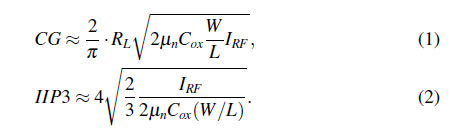
In these formulas, $R_L$ represents the load resistance, while
$I_{RF}$ is the drain current of the RF transistors. The constant
$μ_n$ represents the electron mobility of the transistor, $C_{ox}$
is the gate oxide capacitance, and W and L represent the
width and length of the transistor.
According to Eqs. (1) and (2), both IIP3 and the conversion
gain are proportional to the square root of the bias
current. Thus, increasing the bias current is a straightforward
way to improve linearity and gain. However, in practice,
increasing the bias current results in a higher voltage
drop across the load resistance ($R_L$), which could disrupt
the proper functioning of the switching transistors. Specifically,
when the supply voltage ($V_{DD}$) is fixed, increasing
the bias current requires reducing the load resistance
to maintain the bias conditions of the switching devices,
which in turn reduces the conversion gain. Therefore, to enhance both linearity and gain, it is more effective to increase
$I_{RF}$ without changing the drain-source current of
the switching transistors.
The proposed current-bleeding technique can address
the aforementioned issue. In Fig. 1(a), a bleeding current
source ($I_{BLD}$) is added to the core of a single-balanced
mixer. Without $I_{BLD}$, the total bias current is given by
By introducing $I_{BLD}$, the bias current can be increased
without changing $I_{D1}$ or $I_{D2}$
The presented approach improves both linearity and
conversion gain simultaneously
III. MIXER CIRCUIT DESIGN▼
Fig. 2 shows the schematic of proposed mixer, and Table
1 presents device dimension. The design of a mixer
for superconducting qubit read-out requires careful consideration
of power efficiency, linearity, and noise performance.
Therefore, this section focuses on the implementation
of bleeding transistors and cross-couple techniques
to improve linearity and noise characteristics based on
the conventional double-balanced mixer presented in Fig.
1(b).
The proposed mixer follows a double-balanced architecture,
which is commonly used in RF applications due
to its superior rejection for low local oscillator (LO) leakage
[6]. The core components of the mixer include a pair
of switching transistors that modulate the RF input signal
with the LO signal. The output is taken after the downconversion,
where the difference between the RF and LO
frequencies is obtained.
The cross-coupled current bleeding technique effectively
enhances the CG and noise performance compared to conventional current bleeding mixers. This technique
employs cross-coupled PMOS switches to regulate the
current of the switching transistors, activating at the LO
zero-crossing to supply DC current. As a result, it maintains
the transconductance (gm) of the active switching
transistors while reducing both thermal noise and flicker
noise (1/ f ). Furthermore, the positive feedback effect
of the cross-coupled structure enhances stability while
further increasing conversion gain. Consequently, while
maintaining the same level of noise contribution from the
input source resistance as in conventional double-balanced
mixer, this technique significantly minimizes the noise
impact from the switching, bleeding, and load stages.
Therefore, the cross-coupled current bleeding technique
is highly suitable for high-gain, low-noise mixer designs
[7].
In the design, complementary metal oxide semiconductor
(CMOS) technology is utilized, taking advantage of its
low power consumption and scalability. The input stage
consists of a transconductance amplifier that converts the
RF voltage into a current, which is then mixed with the
LO signal by the switching pair. The LO signal drives
the mixer transistors, ensuring high conversion gain while
minimizing signal distortion.
A critical challenge in the design of mixers for quantum
computing applications is achieving high linearity without sacrificing power efficiency. Nonlinearities in the mixer
can introduce the intermodulation distortion, which affects
the fidelity of qubit read-out. To address this issue,
we introduce bleeding transistors into the mixer architecture.
These transistors serve to maintain a constant current
through the switching pair, reducing the variation in the
LO current during operation. As a result, the linearity of
the mixer is significantly improved.
The bleeding transistors are biased in such a way that
they allow a small, steady current to flow through the
switching transistors even when the LO signal is not actively
switching [8]. This reduces the impact of LO signal
fluctuations, thereby improving the overall linearity of the
mixer. Additionally, the introduction of bleeding transistors
helps to mitigate flicker noise, which is particularly
important in quantum applications where noise minimization
is crucial.
The proposed mixer is designed for minimized power
consumption, which is a key requirement for scalable
quantum computing systems [9]. By operating at only
1.8 mW, the mixer consumes significantly less power
compared to conventional designs, as shown in the performance
comparison in Table 2. This low power consumption
is achieved by optimizing the biasing of the transistors
and carefully selecting the operating points of both the RF
input stage and the LO switching pair.
In terms of noise performance, the use of bleeding transistors
contributes to a lower overall noise figure by reducing
flicker noise and thermal noise contributions. The
wide bandwidth of 4-8GHz ensures that the mixer can
accommodate a broad range of qubit read-out frequencies,
making it highly versatile for various quantum computing
applications.
Schematic of proposed mixer.
Comparison of mixer with proposed mixer.
IV. SIMULATION RESULTS
▼
In this section, we present the post-layout simulation results
of the proposed mixer designed for superconducting
qubit read-out. The performance of the mixer is evaluated
based on key metrics such as conversion gain, noise figure,
linearity, and power consumption. Simulation data are
analyzed to demonstrate the effectiveness of the bleeding
transistors and the overall design.
In RF applications, a higher conversion gain is preferred
to ensure sufficient signal levels for further processing.
The simulation results, as shown in Fig. 3, demonstrate
that the mixer achieves a gain of 16.8 dB at 6 GHz, 10
dB at 4 GHz, and 12 dB at 8 GHz. Fig. 3(a) illustrates the
conversion gain across the 4-8 GHz, while Fig. 3(b) shows
the conversion gain behavior with varying temperatures,
confirming that the mixer operates effectively even in lowtemperature
environments. The use of bleeding transistors
contributes to the stability of the conversion gain, espe-cially at higher frequencies, where traditional designs often
experience degradation.
At 6 GHz, the noise figure reaches approximately 8.6
dB. The bleeding transistors play a significant role in reducing
flicker noise, contributing to the overall low noise
performance. Fig. 4 shows the noise figure of the mixer,
where Fig. 4(a) illustrates the noise figure across different
frequencies, and Fig. 4(b) presents the noise figure as a
function of temperature. In typical superconducting qubit
readout systems, achieving a noise figure (NF) below 1 dB
at temperatures under 4 K is crucial. The readout chain
generally begins with a Josephson parametric amplifier
(JPA) providing approximately 20 dB of gain. Following
this, a High Electron Mobility Transistor (HEMT) amplifies
the signal by an additional 20-30 dB before it reaches
the CMOS-based read-out circuit. The first stage of this
circuit incorporates a low-noise amplifier (LNA). According
to Friis equation, if the mixer’s NF remains below 30
dB, its impact on the overall system NF is minimal, contributing
less than 0.1 dB. As a result, the NF of the mixer is not at the sufficient level in the design.
Linearity is a critical parameter for maintaining the integrity
of the qubit signal [10] proposed design achieves a
1 dB compression point (P1dB) of -11.7 dBm and an IIP3
of -1.2 dBm in simulations, which are considered high for
a low-power mixer. Fig. 5 shows the P1dB and IIP3 of the
mixer. The bleeding transistors help maintain high linearity
by stabilizing the current through the switching pair, as discussed in Section 2.
The circuit to read the qubits existing at 10 mK is typically
located at an ultra-low temperature of 4 K. The cooling
capacity limit at the 4 K stage in a dilution refrigerator
is 1-1.5 W. The capacity of the system to read about 8
qubits should be less than 20 mW/qubit. Therefore, it is
essential to reduce the power consumption of the system,
and the proposed mixer consumes only 1.8 mW. This is
a significant improvement over existing designs that typically
consume higher power at similar performance levels
[11]. Table 3 shows the power consumption as a function
of temperature, and Fig. 6 shows the layout of the proposed
mixer.
Table 4 provides a comparison of the proposed mixer with other state-of-the-art designs. As shown, the proposed
mixer offers competitive performance in terms of
conversion gain, noise figure, and linearity while consuming
significantly less power. The incorporation of bleeding
transistors distinguishes this design by enhancing both
linearity and noise performance, making it well-suited for
quantum computing applications.
Conversion gain of the proposed mixer: (a) conversion
gain vs. frequency, and (b) conversion gain vs. temperature.
Noise figure of the mixer: (a) noise figure vs. frequency,
and (b) noise figure vs. temperature.
P1dB of the mixer: (a) P1dB & IIP3 vs. frequency, and
(b) P1dB vs. temperature.
Layout of proposed mixer.
Power consumption of the according to temperature.
Performance comparison table.
V. CONCLUSIONS
▼
In this paper, we presented the design and implementation
of a 1.8 mW low-power mixer with a 4-8 GHz bandwidth,
specifically developed for superconducting qubit
read-out. By integrating bleeding transistors into the mixer
architecture, the proposed de-sign achieves significant improvements
in linearity and noise performance, both of
which are critical for the precise detection of quantum
states. The mixer’s low power consumption, wide bandwidth,
and robust linearity make it a promising candidate
for use in large-scale quantum computing systems where
energy efficiency and performance are paramount.
Simulation results demonstrate that the mixer achieves
a conversion gain of approximately 16.7 dB with a low
noise figure of 8.6 dB, maintaining competitive performance
in comparison to state-of-the-art designs. The implementation
of bleeding transistors reduces flicker noise
and enhances linearity, yielding an P1dB of up to -11.7
dBm. Moreover, the mixer operates with minimal power
consumption, meeting the stringent requirements of quantum
computing applications.
ACKNOWLEDGMENTS
▼
This research was funded by the National Research
Foundation of Korea (NRF) grant funded by Korean Government
(MIST) (No. 2022R1A4A3029433 and No. RS-
2025-00516839).
References
▼
S. T. Marella and S. K. P. Hemanth, “Introduction to quantum
computing,” Quantum Computing and Communications,
2020.
M. Martonosi and M. Roetteler, “Next steps in quantum
computing: Computer science’s role,”
arXiv preprint
arXiv:1903.10541, 2019.
[
CrossRef]
M. Kjaergaard, M. E. Schwartz, J. Braumüller, P. Krantz,
J. I.-J. Wang, S. Gustavsson, and W. D. Oliver, “Superconducting
qubits: Current state of play,”
Annual Review of Condensed Matter Physics, vol. 11, no. 1, pp. 369-395,
2020.
[
CrossRef]
H.-S. Chang, K. J. Satzinger, Y. P. Zhong, A. Bienfait, M.
H. Chou, C. R. Conner, É. Dumur, J. Grebel, G. A. Peairs,
R. G. Povey, and A. N. Cleland, “A fast and large bandwidth
superconducting variable coupler,”
Applied Physics
Letters, vol. 117, no. 24, 244001, 2020.
[
CrossRef]
S. Douss, F. Touati, and M. Loulou, “A 3.1-4.8 GHz CMOS
mixer design using current bleeding technique for UWB
MB-OFDM receivers,”
Proc. of 2007 IEEE International
Conference on Signal Processing and Communications,
IEEE, 2007.
[
CrossRef]
E. Rubiola, “Tutorial on the double balanced mixer,”
arXiv
preprint physics/0608211 (2006).
[
CrossRef]
H. Darabi and J. Chiu, “A noise cancellation technique in
active RF-CMOS mixers,”
IEEE Journal of Solid-state Circuits,
vol. 40, no. 12, pp. 2628-2632, 2005.
[
CrossRef]
J. Yoon, H. Kim. C. Park, J. Yang, H. Song, and S. Lee,
“A new RF CMOS Gilbert mixer with improved noise figure
and linearity,”
IEEE Transactions on Microwave Theory
and Techniques, vol. 56, no. 3, pp. 626-631, 2008.
[
CrossRef]
J. Ikonen, J. Salmilehto, and M. Möttönen, “Energyefficient
quantum computing,”
npj Quantum Information,
vol. 3, no. 1, 17, 2017.
[
CrossRef]
S. Barz, I. Kassal, M. Ringbauer, Y. O. Lipp, B. Daki´c,
A. Aspuru-Guzik, and P. Walther, “Solving systems of
linear equations on a quantum computer,”
arXiv preprint
arXiv:1302.1210 (2013).
[
CrossRef]
D.-Y. Yoon, S.-J. Yun, J. Cartwright, S.-K. Han, and S.-
G. Lee, “A high gain low noise mixer with cross-coupled
bleeding,”
IEEE Microwave and Wireless Components Letters,
vol. 21, no. 10, pp. 568-570, 2011.
[
CrossRef]
G. H. Tan, R. M. Sidek, M. M. Isa, and S. Shafie, “A lowpower
current bleeding mixer with improved LO-RF isolation
for ZigBee application,”
Proc. of 2013 IEEE International
Conference on Circuits and Systems (ICCAS), IEEE,
2013.
[
CrossRef]
H.-M. Hsu and T.-H. Lee, “High isolation of zero-IF mixer
0.18 um CMOS technology,”
Analog Integrated Circuit
Signal Processing, vol. 49, no.1, pp. 19-25, October 2006.
[
CrossRef]
V. Vidokovic and V. D. Tang, “A low-voltage foldedswitching
in 0.18-μmCMOS,”
IEEE Journal of Solid-State
Circuits, vol. 40, no. 6, pp. 1259-1264, June 2005.
[
CrossRef]
B. Wei, Y. Dai, J. Wang, T. Matsuoka, and K. Taniguchi,
“Design of a low-voltage CMOS mixer based on variable
load technique,”
IEICE Electronic Express, vol. 7, no. 7,
pp. 473-479, April 2010.
[
CrossRef]
W.-R. Liou, M.-L. Yeh, C.-A. Tsai, and S.-H. Chang, “Design
and implementation of a low-voltage 2.4-GHz CMOS
RF receiver front-end for wireless communication,”
Journal
of Marine Science and Technology, vol. 13, no. 3, pp.
170-175, March 2005.
[
CrossRef]
E. Altuner, I. S. Özo˘guz, and M. B. Yelten, “High-linearity
Gilbert-cell mixer design for cryogenic applications,”
Analog
Integrated Circuits and Signal Processing, vol. 113, no.
2, pp. 249-256, 2022.
[
CrossRef]
저자소개
▼
Seunghyeon Baek
is currently pursuing
a B.S. degree in the Department of Electronic
Engineering from Hanbat National
University, Korea. His interests include
SoC circuit design, such as NFC/RFID
reader chip, etc.
Hyeonsik Ahn
received his B.S. and M.S.
degrees from the Department of Electronic
Engineering, Hanbat National University,
Korea, in 2019 and 2021, respectively. He
is currently pursuing a Ph.D. degree in
the Department of Electronic Engineering
from Hanbat National University, Korea.
His interests include cryogenic circuits for
quantum computer and UWB radar Transceiver.
Muhammad Fakhri Mauludin
received
his B.S. degree in engineering physics
from Telkom University in 2019. He received
his M.S. degree from Hanbat National
University in 2022, where he is
now pursuing a Ph.D degree. His research
focuses on cryogenic CMOS circuits
for quantum computing, including
phase-locked loops for accurate frequency generation and qubit
control/readout circuits, as well as low-power and low-noise analog
circuits for biomedical applications.
Youngwoo Ji
received his B.S. and Ph.D.
degrees in electronic and electrical engineering
from the Pohang University of
Science and Technology (POSTECH), Pohang,
South Korea, in 2013 and 2020, respectively.
From 2020 to 2022, he was
a Post-Doctoral Researcher with the Integrated
Systems Laboratory, ETH Zürich,
Zürich, Switzerland. In 2022, he joined Hanbat National University,
where he is currently an Assistant Professor. His research
interests include subthreshold circuit designs, sensor interface
circuits, and data converters. Dr. Ji is a recipient of the IEEE
International Solid-State Circuits Conference (ISSCC) 2022 Jan
Van Vessem Award for Outstanding European Paper.
Jusung Kim
received his B.S. degree
(Hons.) in electrical engineering from
Yonsei University, Seoul, South Korea,
in 2006 and a Ph.D. degree in electrical
engineering from Texas A&M University,
College Station, TX, USA, in 2011. In
2008, he was an Analog IC Design Engineer
with Texas Instruments, Dallas, TX,
USA, where he designed an RF front-end for multistandard analog
and digital TV silicon tuners. From 2011 to 2015, he worked
with Qualcomm Technologies Inc., San Diego, CA, USA, where
he designed RFIC products for 2G-4G+ cellular systems. From
2015 to 2025, he was with Hanbat National University, Daejeon,
South Korea as a faculty member with the Department
of Electronics Engineering. Since 2025, he is with the division
of electronic and semiconductor engineering at Ewha Womans
University with the rank of professor. His research interests
include broadband wireless links in RF and millimeter-wave frequencies,
analysis of device noise and nonlinearity, design and
fabrication of low-power integrated circuits for communication,
and biomedical applications. He has been a member of the Analog
and Signal Processing Technical Committee of IEEE ISCAS
since 2017. He served as an Associate Editor for IEEE Transactions
on Circuits and Systems II: Express Briefs from 2014 to
2015. He is currently an Associate Editor of IEEE Access.